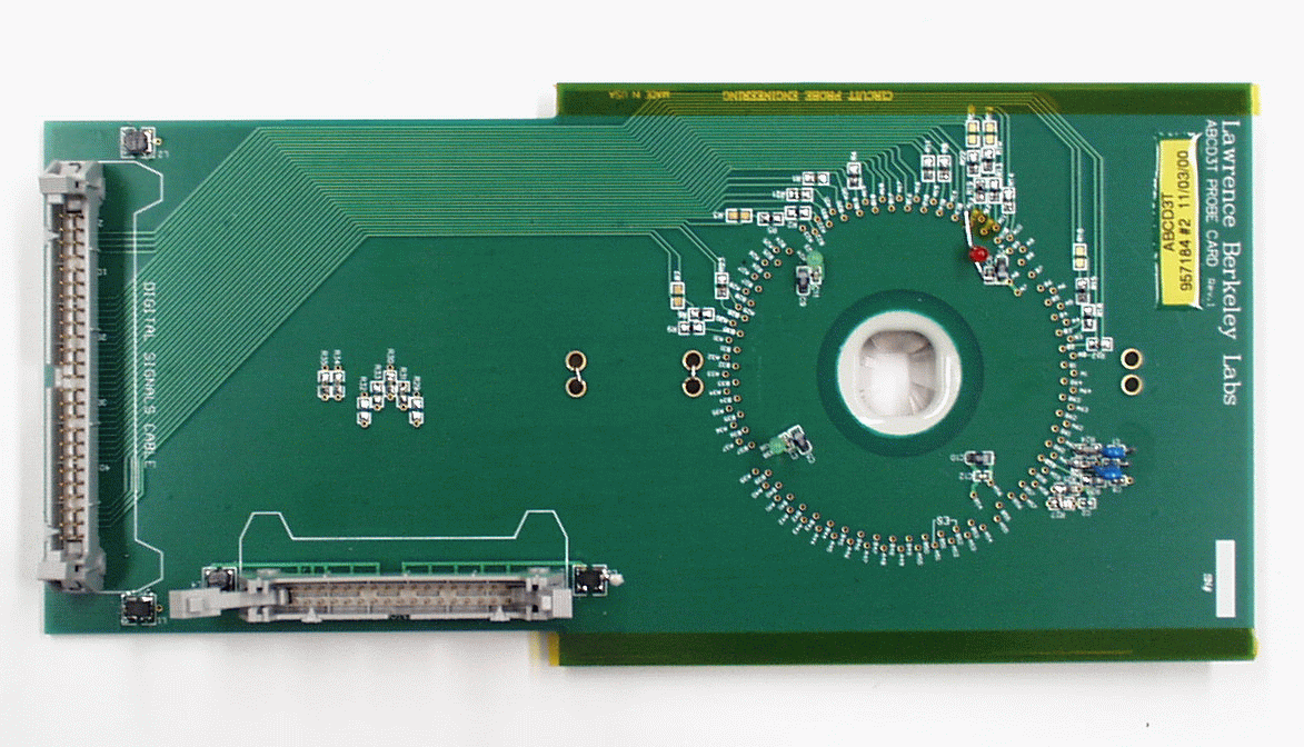
Probe Card
| Prototype | |
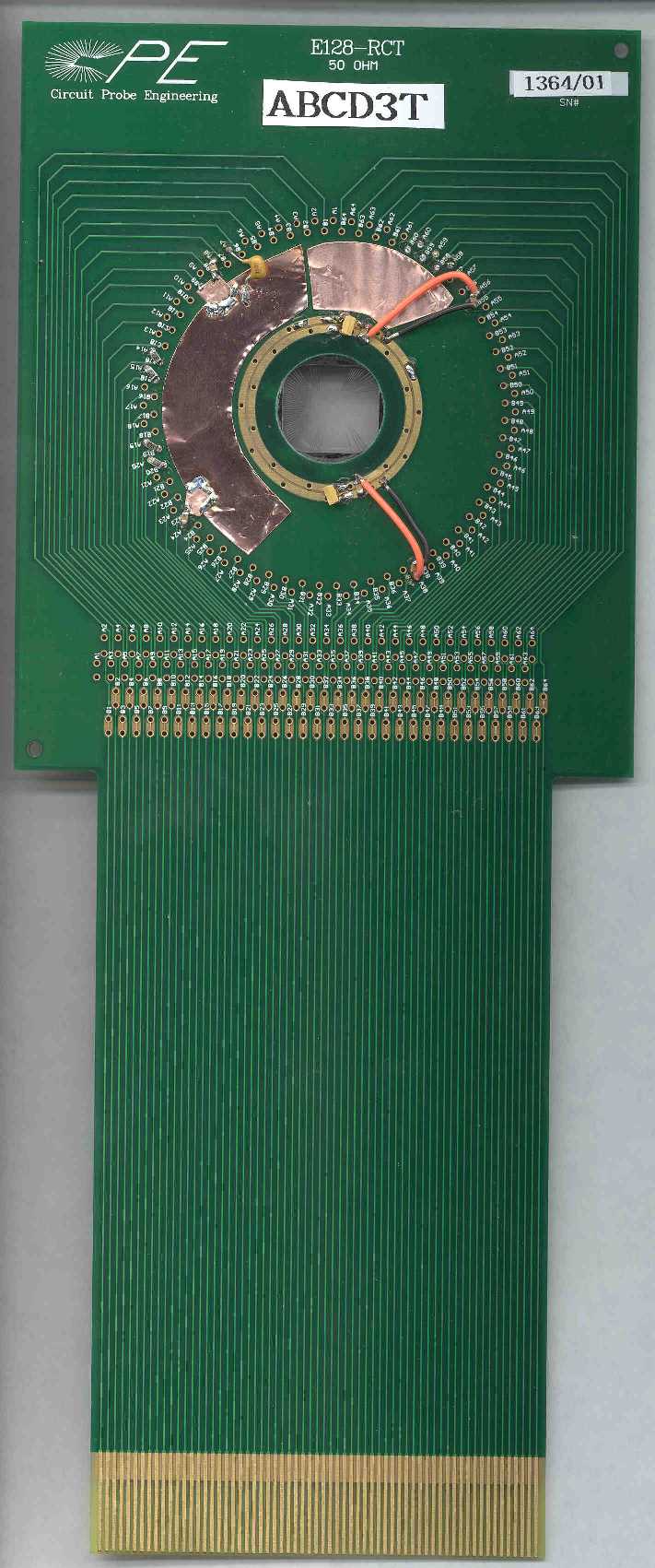
TOP |
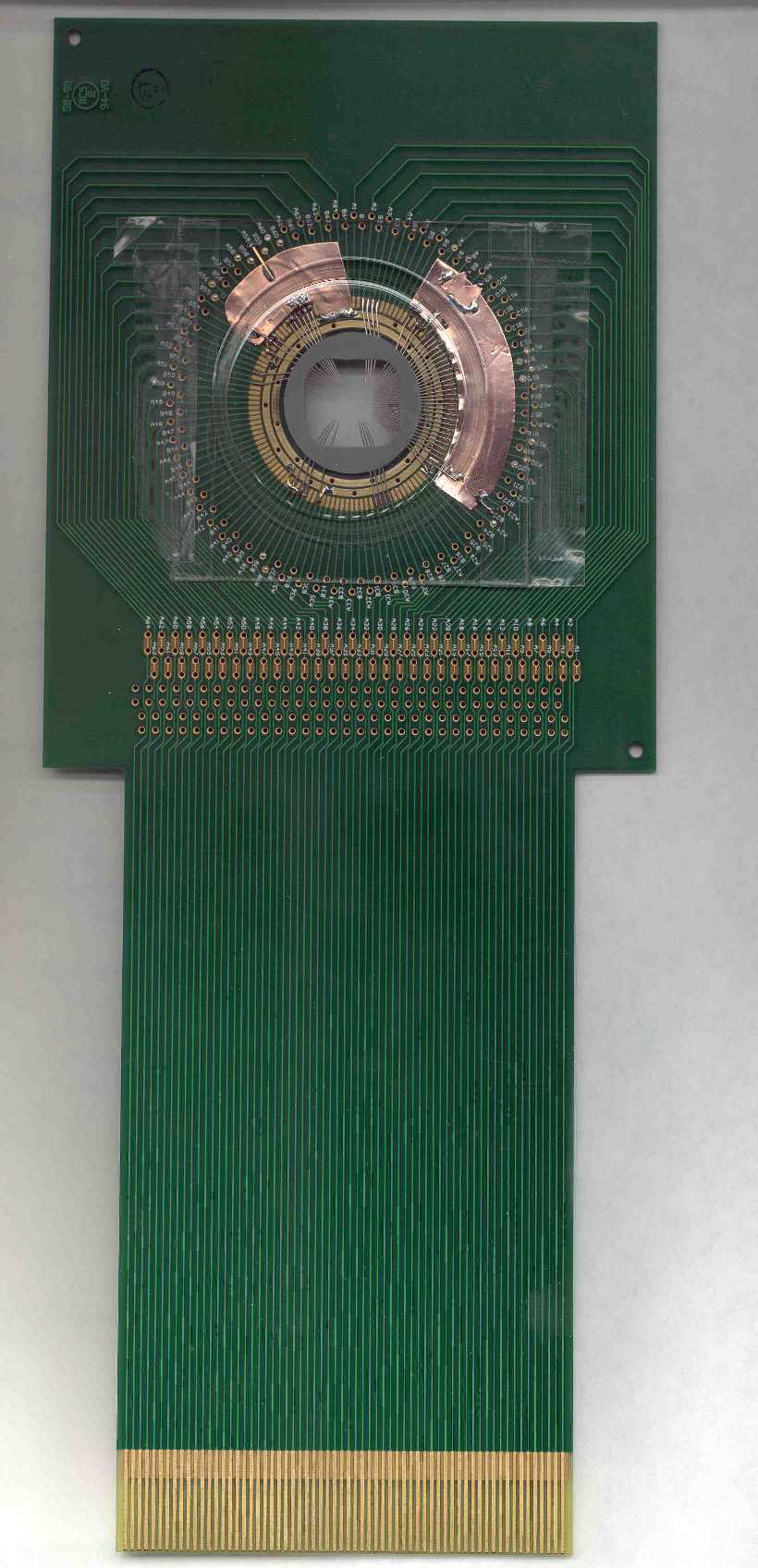
BOTTOM |
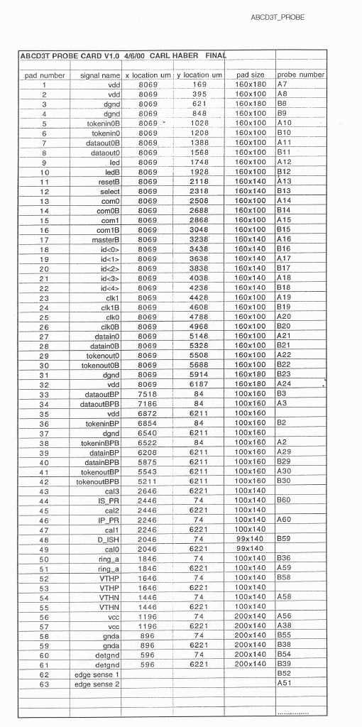
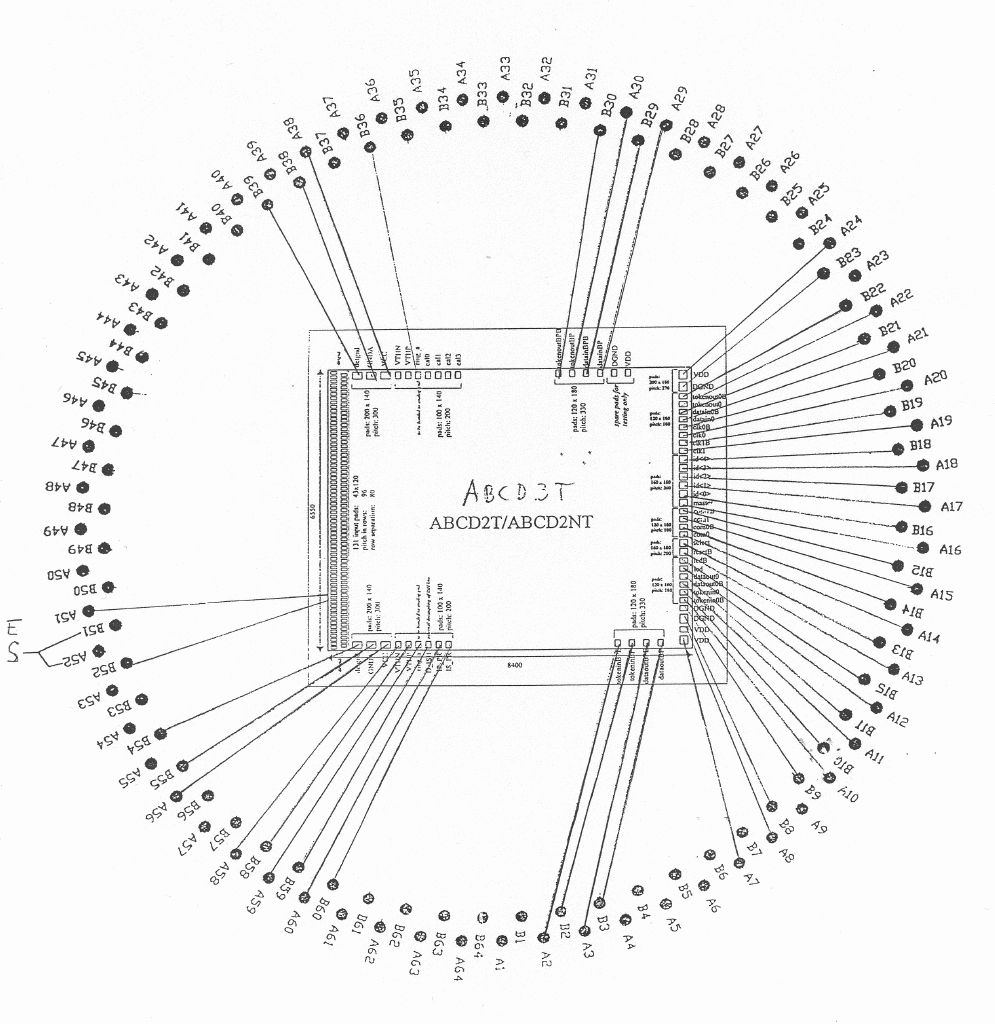
| PINOUT, Connections , and Concard Connector | |
| New layout 6 layers: VCC, VDD, AGND, AGND+DGND connected, Top(B), Bottom(A) |
|
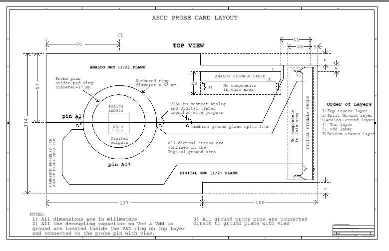
| LAYOUT (AGND + DGND plane) |
| LAYOUT (connectors at right angle) (AGND + DGND plane) |
| LAYOUT (with more details) |
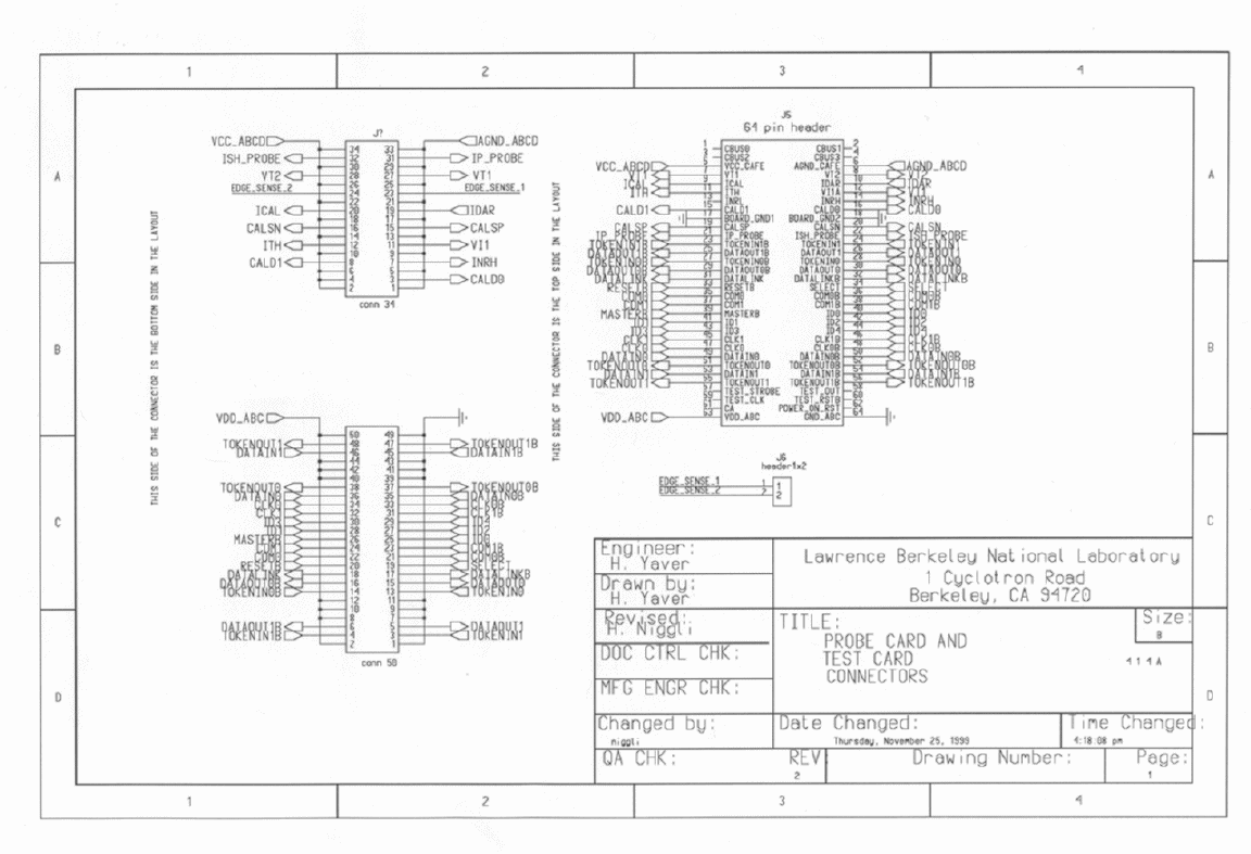
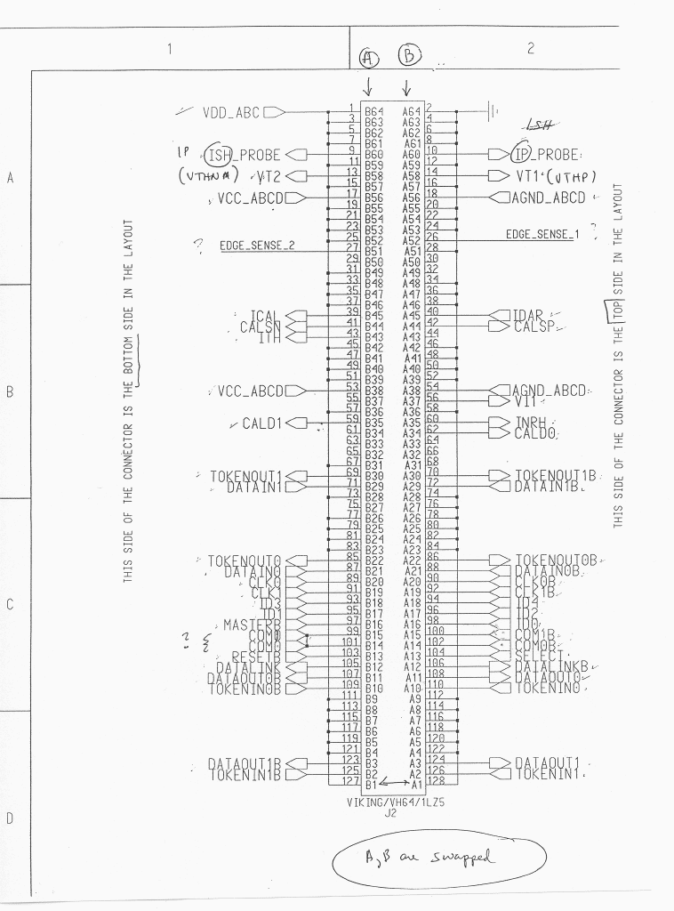
| SCHEMATIC |
| DESCRIPTION doc | pdf |
| BoM |
| New schematic of Connectors on Concard and Probe Card Layout |
|
